


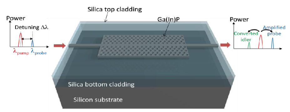
Schematic of basic four-wave mixing measurement in structures made in the embedded Ga(In)P/ substrate platform on SOI.
Integrated photonics has become a viable technology innovation of paramount importance for industrial deployment. Its potential mainly lies in its capacity to handle ever-higher data rates combined to inherently low power operation. Beyond the Internet and telecommunications, integrated photonics may provide a transformational opportunity in other strategic domains (energy, environment, biomedicine…) by possibly enabling the combination of a large variety of optical properties and functionalities on a single chip. However, the number of optical functions presently assembled on a single setting, is still quite limited. In order to enable greater functional integration and enlarge the diversity of implemented optical functions, radically-new direction lines are presently pursued, among which: (i) the extension of nanophotonics to large bandgap material systems, such as GaP, GaN, AlN or diamond, enabling new functions due to their piezoelectric properties, high nonlinear coefficient or biocompatibility, (ii) the integration of III-V compound semiconductor materials-based nanophotonic devices on Si, providing a unique opportunity to combine the advantages of direct bandgap active semiconductor materials with the capabilities of established silicon technologies or (iii) the implementation of disruptive concepts based on the blend of photonics and mechanics on a common chip, paving the way to novel compact information and communication technology optomechanically-driven devices.
These three direction lines will constitute the three main axes of the present flagship. More precisely, the challenges are: (i) to realize diamond-based label-free optical biosensors, by combining the high sensitivity provided by photonic crystal resonators and the advanced bio-functionalization allowed by the chemical versatility of the diamond surface; (ii) to produce phase-sensitive amplifiers and frequency comb sources, by implementing highly non-linear III-V semiconductor devices heterogeneously integrated on Silicon; (iii) to realize integrated optomechanically-driven microwave oscillators.
CONDOR is a highly multidisciplinary and multi-physics project. The consortium gathers unique expertise in diamond and semiconductor growth for nanophotonics, nanotechnologies, non-linear nanophotonics, nano-optomechanics, microwave photonics. The overall expertise is covered by a collaboration of four partners: Laboratoire de Photonique et de Nanostructures, Institut d'Electronique Fondamentale, Laboratoire Capteur Diamant, Thales Research and Technology. It bridges the gap between academic research and industrial technology transfer, through the involvement of 3 academic laboratories and one industrial partner. CONDOR spin-offs do not restrict to biosensing, phase-sensitive amplifiers, frequency comb sources or microwave oscillators. The results of this project will resonate in various areas such as metrology and force sensors, optical treatment of advanced on-chip signal, optical neuromorphic architectures, quantic information optics and processing....
Contact: , LPN
